15 APRIL 2012
It’s time to
itching on PCB. At first, I plan to itching manually, using PCB iron paper and normal
PCB board. But, it is difficult as I don’t have experience doing it by myself
and need to learn the process from the expert. I’m also afraid of doing mistake
that could burn my money; as the iron paper is costly. Finally, I decided to
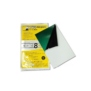
itching on UV board, as it is easier and I can do it at level 1; PCB lab. I can
use the facilities and it is for free. =)
- Photocopy the PCB layout in OHP sheet using laser printer
3. Place board with OHP sheet into a UV exposure unit for
60 second.
4. Wash the developing using ferric chloride. Sink the PCB
in the acid and shake it until the circuit clear from copper; which do not need
on a board.
5. Transfer the PCB in to itching tank and do the operation for 4 minutes; 40˚C onward.
6. After finish on itching tank, scrub the PCB board using sand paper or rub it using thinner liquid. Make sure there is a right connection and continuity on the PCB. Test it using multimeter.
For the first try, after checking the connection and continuity, i found that there is no connection at some point. It is because of my connection line too thin. So, I have to adjust my connection line again; in the DipTrace software, and repeat overall procedure. Here is the result:


